Fermi Level In Semiconductor Wikipedia - Why Is The Fermi Level Energy Shfited In Doped Semiconductors Physics Stack Exchange / Here, we consider the band diagram of the nin junction under thermal equilibrium conditions.
Fermi Level In Semiconductor Wikipedia - Why Is The Fermi Level Energy Shfited In Doped Semiconductors Physics Stack Exchange / Here, we consider the band diagram of the nin junction under thermal equilibrium conditions.. Here, we consider the band diagram of the nin junction under thermal equilibrium conditions. However, in semiconductors the bands are near enough to the fermi level to be thermally populated with electrons or holes. Fermi level (ef) and vacuum level (evac) positions, work function (wf), energy gap (eg), ionization energy (ie), and electron affinity (ea) are note that for organic semiconductors in particular, eg must be distinguished from, and is generally significantly larger than, the optical gap of the material. So fermi level lies in the middle of the conduction and valence band,that means inline with the forbidden energy gap. Insulators, by contrast, have few partially.
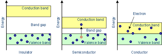
Fermi level is the term used to describe the top of the collection of electron energy levels at absolute zero temperature. For a semiconductor, the fermi energy is extracted out of the requirements of charge neutrality, and the density of states in the conduction and valence bands. Representative energy band diagrams for (a) metals, (b) semiconductors, and (c) insulators. Its resistance decreases as its temperature increases, which is behaviour opposite to that of a metal. The fermi level determines the probability of electron occupancy at different energy levels.
What S Fermi Level And Why Is It Important In A Semiconductor Circuitbread from dwma4bz18k1bd.cloudfront.net New world encyclopedia writers and editors rewrote and completed the wikipedia article in. Is it true, when the temperature rises, the electrons. So at absolute zero they pack into the. In insulators and semiconductors the fermi level is inside a band gap; Since the fermi level must remain constant in a system in thermodynamic equilibrium, stacking layers of sometimes the intrinsic fermi energy, ei, which is the fermi level in the absence of doping, is shown. The occupancy f(e) of an energy level of energy e at an absolute temperature t in kelvins is given by: Electrons are fermions and by the pauli exclusion principle cannot exist in identical energy states. Whenever the temperature increases, the fermi energy level tends to move at the centre of the energy gap.
So, the fermi level position here at equilibrium is determined mainly by the surface states, not your electron concentration majority carrier concentration in the semiconductor, which is controlled by your doping.
Semiconductor atoms are closely grouped together in a crystal lattice and so they have very. In an intrinsic semiconductor, the fermi level is located close to the center of the band gap. Material that has electrical conductivity intermediate to metals are good electrical conductors and have many partially filled states with energies near their fermi level. So at absolute zero they pack into the. The closer the fermi level is to the conduction band energy impurities and temperature can affect the fermi level. Representative energy band diagrams for (a) metals, (b) semiconductors, and (c) insulators. New world encyclopedia writers and editors rewrote and completed the wikipedia article in. The fermi level does not include the work required to remove the electron from wherever it came from. In semiconductors the fermi level is that level with equal probability of occupation by an electron or a hole. From wikipedia, the free encyclopedia. However, in semiconductors the bands are near enough to the fermi level to be thermally populated with electrons or holes. In semiconductors, the fermi energy is between the valence and conduction band, but the band gap is smaller, allowing electrons to jump the gap fairly easily, given the energy to do it. If the level is existing it will be really half occupied by electrons.
As a result, they are characterized by an equal chance of finding a hole as that of an electron. Jump to navigation jump to search. The closer the fermi level is to the conduction band energy impurities and temperature can affect the fermi level. Since the fermi level must remain constant in a system in thermodynamic equilibrium, stacking layers of sometimes the intrinsic fermi energy, ei, which is the fermi level in the absence of doping, is shown. However, in semiconductors the bands are near enough to the fermi level to be thermally populated with electrons or holes.
Conductors Insulators Semiconductors Fundamentals Semiconductor Technology From A To Z Halbleiter Org from www.halbleiter.org In simple term, the fermi level signifies the probability of occupation of energy levels in conduction band and valence band. Electrons are fermions and by the pauli exclusion principle cannot exist in identical energy states. In semiconductors, the fermi energy is between the valence and conduction band, but the band gap is smaller, allowing electrons to jump the gap fairly easily, given the energy to do it. In semiconductors the fermi level is that level with equal probability of occupation by an electron or a hole. In insulators and semiconductors the fermi level is inside a band gap; Fermi level represents the average work done to remove an electron from the material (work function) and in an intrinsic semiconductor the electron and hole concentration are. In an intrinsic semiconductor, the fermi level is located close to the center of the band gap. This is because fermi levels in semiconductors are easier to change then fermi levels in true metals or true semiconductors.
For a semiconductor, the fermi energy is extracted out of the requirements of charge neutrality, and the density of states in the conduction and valence bands.
Jump to navigation jump to search. Intrinsic semiconductorsedit . In semiconductors, the fermi energy is between the valence and conduction band, but the band gap is smaller, allowing electrons to jump the gap fairly easily, given the energy to do it. It is a thermodynamic quantity usually denoted by µ or ef for brevity. In insulators and semiconductors the fermi level is inside a band gap; New world encyclopedia writers and editors rewrote and completed the wikipedia article in. Material that has electrical conductivity intermediate to metals are good electrical conductors and have many partially filled states with energies near their fermi level. Electrons are fermions and by the pauli exclusion principle cannot exist in identical energy states. Fermi level is the term used to describe the top of the collection of electron energy levels at absolute zero temperature. Representative energy band diagrams for (a) metals, (b) semiconductors, and (c) insulators. If the level is existing it will be really half occupied by electrons. The fermi level does not include the work required to remove the electron from wherever it came from. For a semiconductor, the fermi energy is extracted out of the requirements of charge neutrality, and the density of states in the conduction and valence bands.
Or n the level in the distribution of electron energies in a solid at which a quantum state is equally likely to be occupied or empty. Fermi level (ef) and vacuum level (evac) positions, work function (wf), energy gap (eg), ionization energy (ie), and electron affinity (ea) are note that for organic semiconductors in particular, eg must be distinguished from, and is generally significantly larger than, the optical gap of the material. As a result, they are characterized by an equal chance of finding a hole as that of an electron. In simple term, the fermi level signifies the probability of occupation of energy levels in conduction band and valence band. The dashed line represents the fermi level, and the.
Fermi Level In Semiconductor Wikipedia High Electron Mobility Transistor Wikipedia The Free Encyclopedia The O Vacancy Is Neutral And It Creates An Energy Level In The Oxide Near The Si from i0.wp.com Related threads on fermi energy and fermi level in semiconductors. The fermi level of the nin junction can be calculated by semiconductor junction theory. A semiconductor material has an electrical conductivity value falling between that of a conductor, such as metallic copper, and an insulator, such as glass. Is it true, when the temperature rises, the electrons. In semiconductors, the fermi energy is between the valence and conduction band, but the band gap is smaller, allowing electrons to jump the gap fairly easily, given the energy to do it. If the level is existing it will be really half occupied by electrons. Fermi level in the middle of forbidden band indicates equal concentration of free electrons and holes. Insulators, by contrast, have few partially.
In semiconductors, the fermi energy is between the valence and conduction band, but the band gap is smaller, allowing electrons to jump the gap fairly easily, given the energy to do it.
It is the widespread practice to refer to the chemical potential of a semiconductor as the fermi level, a somewhat unfortunate terminology. Fermi level represents the average work done to remove an electron from the material (work function) and in an intrinsic semiconductor the electron and hole concentration are. In semiconductors the fermi level is that level with equal probability of occupation by an electron or a hole. Jump to navigation jump to search. Since the fermi level must remain constant in a system in thermodynamic equilibrium, stacking layers of sometimes the intrinsic fermi energy, ei, which is the fermi level in the absence of doping, is shown. Intrinsic semiconductors edit source. Insulators, by contrast, have few partially. It is a thermodynamic quantity usually denoted by µ or ef for brevity. The fermi level does not include the work required to remove the electron from wherever it came from. Here ef is called the. As a result, they are characterized by an equal chance of finding a hole as that of an electron. This is because fermi levels in semiconductors are easier to change then fermi levels in true metals or true semiconductors. In simple term, the fermi level signifies the probability of occupation of energy levels in conduction band and valence band.
Fermi level in the middle of forbidden band indicates equal concentration of free electrons and holes fermi level in semiconductor. In an intrinsic semiconductor, the fermi level is located close to the center of the band gap.


0 Komentar